Pages

Sunday, July 29, 2012

22 Watt Audio Amplifier Circuit

The 22 watt amp is easy to build, and very inexpensive. The circuit can be used as a booster in a car audio system, an amp for satellite speakers in a surround sound or home theater system, or as an amp for computer speakers. The circuit is quite compact and uses only about 60 watts. The circuit is not mine, it came from Popular Electronics.
Circuit diagram
22 Watt Audio Amplifier Circuit
Parts
R1 39K 1/4 Watt Resistor
C1,C2 10uf 25V Electrolytic Capacitor
C3 100uf 25V Electrolytic Capacitor
C4 47uf 25V Electrolytic Capacitor
C5 0.1uf 25V Ceramic Capacitor
C6 2200uf 25V Electrolytic Capacitor
U1 TDA1554 Two Channel Audio Amp Chip
MISC Heatsink For U1, Binding Posts (For Output), RCA Jacks (For Input), Wire, Board
Notes
1. The circuit works best with 4 ohm speakers, but 8 ohm units will do.
2. The circuit dissipates roughly 28 watts of heat, so a good heatsink is necessary. The chip should run cool enough to touch with the proper heatsink installed.
3. The circuit operates at 12 Volts at about 5 Amps at full volume. Lower volumes use less current, and therefore produce less heat.
4. Printed circuit board is preferred, but universal solder or perf board will do. Keep lead length short.

18W Audio Amplifier Circuit

circuit diagram
18W Audio Amplifier Circuit
Amplifier parts:
P1 = 22K Log.Potentiometer (Dual-gang for stereo)
R1 = 1K 1/4W Resistor
R2 = 4K7 1/4W Resistor
R3 = 100R 1/4W Resistor
R4 = 4K7 1/4W Resistor
R5 = 82K 1/4W Resistor
R6 = 10R 1/2W Resistor
R7 = R22 4W Resistor (wire wound)
R8 = 1K 1/2W Trimmer Cermet (optional)
C1 = 470nF 63V Polyester Capacitor
C2,C5 = 100uF 3V Tantalum bead Capacitors
C3,C4 = 470uF 25V Electrolytic Capacitors
C6 = 100nF 63V Polyester Capacitor
D1 = 1N4148 75V 150mA Diode
IC1 = TLE2141C Low noise,high voltage,high slew-rate Op-amp
Q1 = BC182 50V 100mA NPN Transistor
Q2 = BC212 50V 100mA PNP Transistor
Q3 = TIP42A 60V 6A PNP Transistor
Q4 = TIP41A 60V 6A NPN Transistor
J1 RCA audio input socket
Power supply parts:
R9 = 2K2 1/4W Resistor
C7,C8 = 4700uF 25V Electrolytic Capacitors
D2 100V 4A Diode bridge
D3 5mm. Red LED
T1 220V Primary, 15 + 15V Secondary 50VA Mains transformer
PL1 Male Mains plug
SW1 SPST Mains switch
Notes:
Can be directly connected to CD players, tuners and tape recorders.
Don't exceed 23 + 23V supply.
Q3 and Q4 must be mounted on heat sink.
D1 must be in thermal contact with Q1.
Quiescent current (best measured with an Avo-meter in series with Q3 Emitter) is not critical.
Adjust R3 to read a current between 20 to 30 mA with no input signal.
To facilitate current setting add R8 (optional).
A correct grounding is very important to eliminate hum and ground loops. Connect in the same point the ground sides of J1, P1, C2, C3 &C4. Connect C6 at the output ground.
Then connect separately the input and output grounds at the power supply ground.
Technical data:
Output power: 18 Watt RMS @ 8 Ohm (1KHz sine wave)
Sensitivity: 150mV input for 18W output
Frequency response: 30Hz to 20KHz -1dB
Total harmonic distortion @ 1KHz: 0.1W 0.02% 1W 0.01% 5W 0.01% 10W 0.03%
Total harmonic distortion @10KHz: 0.1W 0.04% 1W 0.05% 5W 0.06% 10W 0.15%
Unconditionally stable on capacitive loads
Author:
website: http://www.redcircuits.com/

10W Mini Audio Amplifier Circuit

finished device
10W Mini Audio Amplifier Circuit
Componets Layout

PCB

Componets List
R1 : 6 Ohm
R2 : 220 Ohm
R3 : nothing
R4 : 10 KOhm pontesiometer
C1 : 2200 uF / 25V
C2 : 470 uF / 16V
C3 : 470 nF / 63V
C4 : 100 nF
C5 : nothing
C6 : nothing
IC1 : TDA 2003
Author:
website: http://www.electronics-lab.com/

60W Bass Amplifier Circuit

Low-cut and Bass controls
Output power: 40W on 8 Ohm and 60W on 4 Ohm loads
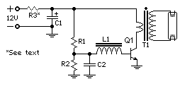
Amplifier circuit diagram:
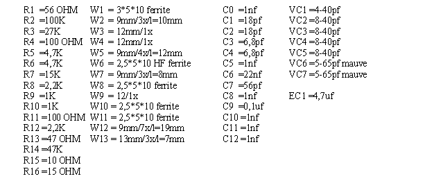
60W Bass Amplifier Circuit
Amplifier parts:
R1 6K8 1W Resistor
R2,R4 470R 1/4W Resistors
R3 2K 1/2W Trimmer Cermet
R5,R6 4K7 1/2W Resistors
R7 220R 1/2W Resistor
R8 2K2 1/2W Resistor
R9 50K 1/2W Trimmer Cermet
R10 68K 1/4W Resistor
R11,R12 R47 4W Wirewound Resistors
C1,C2,C4,C5 47�F 63V Electrolytic Capacitors
C3 100�F 25V Electrolytic Capacitor
C6 33pF 63V Ceramic Capacitor
C7 1000�F 50V Electrolytic Capacitor
C8 2200�F 63V Electrolytic Capacitor (See Notes)
D1 LED Any type and color
D2 Diode bridge 200V 6A
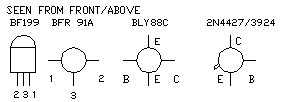
Q1,Q2 BD139 80V 1.5A NPN Transistors
Q3 MJ11016 120V 30A NPN Darlington Transistor (See Notes)
Q4 MJ11015 120V 30A PNP Darlington Transistor (See Notes)
SW1 SPST Mains switch
F1 4A Fuse with socket
T1 220V Primary, 48-50V Secondary 75 to 150VA Mains transformer
PL1 Male Mains plug
SPKR One or more speakers wired in series or in parallel. Total resulting impedance: 8 or 4 Ohm. Minimum power handling: 75W
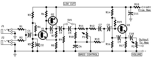
Preamplifier circuit diagram:

Preamplifier parts:
P1 10K Linear Potentiometer
P2 10K Log. Potentiometer
R1,R2 68K 1/4W Resistors
R3 680K 1/4W Resistor
R4 220K 1/4W Resistor
R5 33K 1/4W Resistor
R6 2K2 1/4W Resistor
R7 5K6 1/4W Resistor
R8,R18 330R 1/4W Resistors
R9 47K 1/4W Resistor
R10 18K 1/4W Resistor
R11 4K7 1/4W Resistor
R12 1K 1/4W Resistor
R13 1K5 1/4W Resistor
R14,R15,R16 100K 1/4W Resistors
R17 10K 1/4W Resistor
C1,C4,C8,C9,C10 10�F 63V Electrolytic Capacitors
C2 47�F 63V Electrolytic Capacitor
C3 47pF 63V Ceramic Capacitor
C5 220nF 63V Polyester Capacitor
C6 470nF 63V Polyester Capacitor
C7 100nF 63V Polyester Capacitor
C11 220�F 63V Electrolytic Capacitor
Q1,Q3 BC546 65V 100mA NPN Transistors
Q2 BC556 65V 100mA PNP Transistor
J1,J2 6.3mm. Mono Jack sockets
SW1 SPST Switch
Circuit description:
This design adopts a well established circuit topology for the power amplifier, using a single-rail supply of about 60V and capacitor-coupling for the speaker(s). The advantages for a guitar amplifier are the very simple circuitry, even for comparatively high power outputs, and a certain built-in degree of loudspeaker protection, due to capacitor C8, preventing the voltage supply to be conveyed into loudspeakers in case of output transistors' failure.
The preamp is powered by the same 60V rails as the power amplifier, allowing to implement a two-transistors gain-block capable of delivering about 20V RMS output. This provides a very high input overload capability.
Technical data:
Sensitivity:
70mV input for 40W 8 Ohm output
63mV input for 60W 4 Ohm output
Frequency response:
50Hz to 20KHz -0.5dB; -1.5dB @ 40Hz; -3.5dB @ 30Hz
Total harmonic distortion @ 1KHz and 8 Ohm load:
Below 0.1% up to 10W; 0.2% @ 30W
Total harmonic distortion @ 10KHz and 8 Ohm load:
Below 0.15% up to 10W; 0.3% @ 30W
Total harmonic distortion @ 1KHz and 4 Ohm load:
Below 0.18% up to 10W; 0.4% @ 60W
Total harmonic distortion @ 10KHz and 4 Ohm load:
Below 0.3% up to 10W; 0.6% @ 60W
Bass control:
Fully clockwise = +13.7dB @ 100Hz; -23dB @ 10KHz
Center position = -4.5dB @ 100Hz
Fully counterclockwise = -12.5dB @ 100Hz; +0.7dB @ 1KHz and 10KHz
Low-cut switch:
-1.5dB @ 300Hz; -2.5dB @ 200Hz; -4.4dB @ 100Hz; -10dB @ 50Hz
Notes:
The value listed for C8 is the minimum suggested value. A 3300�F capacitor or two 2200�F capacitors wired in parallel would be a better choice.
The Darlington transistor types listed could be too oversized for such a design. You can substitute them with MJ11014 (Q3) and MJ11013 (Q4) or TIP142 (Q3) and TIP147 (Q4).
T1 transformer can be also a 24 + 24V or 25 + 25V type (i.e. 48V or 50V center tapped). Obviously, the center-tap must be left unconnected.
SW1 switch inserts the Low-cut feature when open.
In all cases where Darlington transistors are used as the output devices it is essential that the sensing transistor (Q2) should be in as close thermal contact with the output transistors as possible. Therefore a TO126-case transistor type was chosen for easy bolting on the heatsink, very close to the output pair.
R9 must be trimmed in order to measure about half the voltage supply from the positive lead of C7 and ground. A better setting can be done using an oscilloscope, in order to obtain a symmetrical clipping of the output waveform at maximum output power.
To set quiescent current, remove temporarily the Fuse F1 and insert the probes of an Avo-meter in the two leads of the fuse holder.
Set the volume control to the minimum and Trimmer R3 to its minimum resistance.
Power-on the circuit and adjust R3 to read a current drawing of about 30 to 35mA.
Wait about 15 minutes, watch if the current is varying and readjust if necessary.
author:RED Free Circuit Designs,
website: http://www.redcircuits.com/

2 Transistor FM Voice Transmitter Circuit

Circuit diagram
2 Transistor FM Voice Transmitter Circuit
Notes:
I have used a pair of BC548 transistors in this circuit. Although not strictly RF transistors, they still give good results. I have used an ECM Mic insert from Maplin Electronics, order code FS43W. It is a two terminal ECM, but ordinary dynamic mic inserts can also be used, simply omit the front 10k resistor. The coil L1 was again from Maplin, part no. UF68Y and consists of 7 turns on a quarter inch plastic former with a tuning slug. The tuning slug is adjusted to tune the transmitter. Actual range on my prototype tuned from 70MHz to around 120MHz. The aerial is a few inches of wire. Lengths of wire greater than 2 feet may damp oscillations and not allow the circuit to work. Although RF circuits are best constructed on a PCB, you can get away with veroboard, keep all leads short, and break tracks at appropriate points.
One final point, don't hold the circuit in your hand and try to speak. Body capacitance is equivalent to a 200pF capacitor shunted to earth, damping all oscillations. I have had some first hand experience of this problem.
author:Andy Collinson,
website: http://www.zen22142.zen.co.uk/

FM Transmitter Bug Circuit

Circuit diagram
FM Transmitter Bug Circuit
Notes:
This small transmitter uses a hartley type oscillator. Normally the capacitor in the tank circuit would connect at the base of the transistor, but at VHF the base emitter capacitance of the transistor acts as a short circuit, so in effect, it still is. The coil is four turns of 18swg wire wound around a quarter inch former. The aerial tap is about one and a half turns from the supply end. Audio sensitivity is very good when used with an ECM type microphone insert
author:David, radio_david@yahoo.com

3W FM Transmitter Circuit

This is the schematic for an FM transmitter with 3 to 3.5 W output power that can be used between 90 and 110 MHz. Although the stability isn't so bad, a PLL can be used on this circuit.
This is a circuit that I've build a few years ago for a friend, who used it in combination with the BLY88 amplifier to obtain 20 W output power. From the notes that I made at the original schematic, it worked fine with a SWR of 1 : 1.05 (quite normal at my place with my antenna).

Circuit diagram
3W FM Transmitter Circuit

Parts:
R1,R4,R14,R15 10K 1/4W Resistor
R2,R3 22K 1/4W Resistor
R5,R13 3.9K 1/4W Resistor
R6,R11 680 Ohm 1/4W Resistor
R7 150 Ohm 1/4W Resistor
R8,R12 100 Ohm 1/4W Resistor
R9 68 Ohm 1/4W Resistor
R10 6.8K 1/4W Resistor
C1 4.7pF Ceramic Disc Capacitor
C2,C3,C4,C5,C7,C11,C12 100nF Ceramic Disc Capacitor
C6,C9,C10 10nF Ceramic Disc Capacitor
C8,C14 60pF Trimmer Capacitor
C13 82pF Ceramic Disc Capacitor
C15 27pF Ceramic Disc Capacitor
C16 22pF Ceramic Disc Capacitor
C17 10uF 25V Electrolytic Capacitor
C18 33pF Ceramic Disc Capacitor
C19 18pF Ceramic Disc Capacitor
C20 12pF Ceramic Disc Capacitor
C21,C22,C23,C24 40pF Trimmer Capacitor
C25 5pF Ceramic Disc Capacitor
L1 5 WDG, Dia 6 mm, 1 mm CuAg, Space 1 mm
L2,L3,L5,L7,L9 6-hole Ferroxcube Wide band HF Choke (5 WDG)
L4,L6,L8 1.5 WDG, Dia 6 mm, 1 mm CuAg, Space 1 mm
L10 8 WDG, Dia 5 mm, 1 mm CuAg, Space 1 mm
D1 BB405 or BB102 or equal (most varicaps with C = 2-20 pF [approx.] will do)
Q1 2N3866
Q2,Q4 2N2219A
Q3 BF115
Q5 2N3553
U1 7810 Regulator
MIC Electret Microphone
MISC PC Board, Wire For Antenna, Heatsinks

Notes:
1. Email Rae XL Tkacik with questions, comments, etc.
2. The circuit has been tested on a normal RF-testing breadboard (with one side copper). Make some connections between the two sides. Build the transmitter in a RF-proof casing, use good connectors and cable, make a shielding between the different stages, and be aware of all the other RF rules of building.
3. Q1 and Q5 should be cooled with a heat sink. The case-pin of Q4 should be grounded.
4. C24 is for the frequency adjustment. The other trimmers must be adjusted to maximum output power with minimum SWR and input current.
5. Local laws in some states, provinces or countries may prohibit the operation of this transmitter. Check with the local authorities.
author:Rae XL Tkacik, vocko@atlas.cz
website: http://www.aaroncake.net/circuits/index.asp

15W Fm-transmitter Circuit

It was five years ago when I did an attempt to build my first fm-transmitter. It ended in a giant faillure. The only thing it did was interferring with our tv-set. Looking back it was due to the lack of information I had. A schematic was my only help. Now, five years later, I know a lot more about electro-technics. So I searched for a schematic of a stable, tested fm-transmitter with a far reach. I will put all information you'll have to know in my page. I made drawings to make things clearer. As said before: I'm still building it, so I will add information every time I made progress. It would be wise for you out there not to start building untill I'm ready and have tested it. It has been succesfully built before, but my succes will give you a double security. I remind you of the fact that I can also fail.

Intro
Building a good fm-transmitter(88-110Mhz) begins with getting a good schematic. You don't have to understand the precise working of the transmitter to build it. But some basic information won't harm. A transmitter alone is, as you probably know, is not enough to start your radio-station. In the simplest form you need 4 things. First an input device such as an amplifiler you also use with your home-stereo.
You can also use a walkman. Details about input-devices in the page: "Input". Second you need a regulated power-supply. In this case a 14-18 Volts/2,5-3,5 Ampere. One of the most influencial things you need is antenna and coax-cable. More about this later on. And finally the transmitter itself. You can devide the transmitter in two main parts: the oscilator and the amplifiler. The oscilator converts electric sound information into electromagnetic waves. The amplifiler gives these waves
a bigger amplitude.

Building
It's stable and has output of 15-18 watts. This enough to terrorize your wide surroundings at the fm-band.
The most often used technique to connect the components to each other is soldering them on a double sided copper-board. Another way is connecting the components floating. It is cheaper but very tricky. Below you see the copper-board layout(PCB). I designed it looking closely at the root scheme.

To get this pattern in copper surface you use a acid bath. Use a water-resistant permanent marker to paint your own copper-board black in the pattern the shown above. Color the back side ompletely black. The grid-squares are 0,5*0,5 cm each.

When the acid has eaten the non-painted copper away you must remove the complet thin layer of black paint with sandpaper. Don't remove too much copper with it.
So, now you have the surface to solder the electric components on.
Now a few basic rules for good soldering:
1. Use a special electronics-solderingrod with a slim top.
2. Use soldering-metal with an anti-oxidant-fluid core.
3. Don't heat the components! Heat the connection-point on your PCB.
4. Make sure that the surface is not too smooth.
5. Don't use too much metal.
6. Don't let the soldering metal form a bridge beetween two copper-surfaces.
7. If you're smart you start from the middle of your prepaired board.
In this way you'll have enough space.
Below the schematic. The yellow lines are pieces of copperboard that devide the transmitter in 3 parts. This is essential. Without them, internal interferrence will ruin your signal.


Parts

There are some components that need extra attention. Transistors usually have 3 or 4 different
wires comin' out. If you connect these wires in the wrong way the transmitter won't work. It may even explode. The picture below shows how to prevent from such an event.

You can find the numbers and letters back in the soldering schematic.
Coils also require extra attention. You can buy the coils trough ferrite in the shop, but the other ones have to be made yourself. Use 1mm AgCu wire. A coil like 7x/d=10mm/l=15mm, goes round 7 times, has an diameter of 10 millimeter and is long 15 millimeters. The best way to make a coil is to bend it around a pencil or other cilindrical shaped object tight. The diameter of the object is always d-coil minus 1 mm. In this case 9mm. As I said: bend the wire round (in this case 7times) with the revolves tight together. To get the desired length stretch the coil when still around the pencil
If you decide to build the transmitter and buy the parts, this list will be handy:
compon.doc
READ THIS E-MAIL I RECEIVED
Hello,
just to give some input: I have built the 15W FM transmitter you describe about 4.5 years ago.
The PCB lay out and component selection is still the same as it was then and after some modifications, I had an average output power of 16.8W @ 98.6 MHz (measured with Rhode and Schwarz equipement). You will need additional filtering on the power lines otherwise a stable power supply for the modulating circuit cannot be guaranteed. The legs of the modulating diode are, at best, kept long for extra capacitance. This to make sure you fall within the FM band because before I did that, I had
problems falling withing the 88-108 MHz. I was actually interfering with the police and fire brigade radio bands (Belgium). Of course, this is not the intention. I also advice you and readers to carefully check the orientation of the BLY88 because my professor blew one up due to lack of specification and inclarities in the datasheets (the actual pin out of the component changed a few years ago, resulting in a swapped emitter and collector - no good if you position it wrong!!! (the white cap flies of)). You will also need to play with the spacing between the windings of the different coils in order to get a good coupling between the different stages. I short circuited parts of the coils and made them smaller than specified to have near-optimal coupling. I also added extra ferrite bead coils for extra decoupling of the power lines, and used a very good shielding. Above 16.8W there is coupling (primarily through the air) between the output and the modulating/input stage and oscillation occurs. So for I have not found any other solution than lower the output power. Both extra decoupling
and extra shielding had no effect (my transmitter is built into a fully closed aluminium box with seperating plates that are fully connected to the case or ground plane on the PCB, except from where tracks run (0.5mm spacing provided)). Also, use a good heat sink for the last power stage!!!
I hope this information will be usefull. If you have any questions, please ask.
Kind regards,
Erwin Huybreghts
Electronic Engineer
Space applications and space instruments division
Verhaert D&D
Belgium
Author:
website: http://www.geocities.com/SouthBeach/3433/transmit.htm

Transmitter FM 45W with valve Circuit

TECHNICAL CHARACTERISTICS:
Tendency of catering: 220V AC
Frequency of emission at FM: 88~108MHz
Force of expense: max 45W (without the R3),
Transmitter FM 45W with valve Circuit
Materially:
R1 15KW/2W
R2 1KW/10W
R3 1KW/10W (for biggest force in the exit you replace with short-circuit).
C1 50pF trimmer
C2 30pF trimmer
C3 22pF/4KV
C4, c6, c9 10nF/1KV
C5, c7 1nF/1KV
C8 100mF+100mF/450V (Double electrolytic)
C9, c10 10nF
RFC1, rfc2, rfc3 air Inductors: 15 coils diameter 8mm, from wire 1mm.
T1 Transformer 220V/6V-1A
T2 Transformer of configuration with being first 4 or 8W
T3 Inductor with core ferrite (externally it resembles with small transformer but has a turn only).
D1 BY127 rectifier
Lamp 807 SYLV USA or EL34 or equivalent
ANTENNA Simple dipole L/2. (L= wave length)
S1 Main switch of catering.
S2 Switch of catering of rise (him we close after zestacej' the thread).
[color=green]Most elements you can him find in a old back-white television with lamps.[/color]
Regulations:
With the C2 we regulate the frequency.
With the C1 we adapt the resistance of aerial (practically him we regulate so that it is heard our voice in the radio as long as you become cleaner).
Notes:
The catering better it does not become at straight line from the network 220V but via transformer 220V/220V of isolation and safety 1A.
When does not exist the R3, the force of expense is bigger, but respectively is increased also the hum 50Hz, because the simplicity of designing.
The control (Audio In) can become from a kasseto'fwno or other powerful source. If it is microphone it will be supposed precedes amplifier so that it acquires a force of order of 8W roughly.
author:Kyriakos Kontakos, kkontak@hotmail.com

4W FM Transmitter Circuit

TECHNICAL CHARACTERISTICS:
Stabilised tendency of catering: Vcc=12~16V
Frequency of emission: 88~108MHz
Consumption: 100~400mA
Circuit diagram:
4W FM Transmitter Circuit
Materially:
[color=green]The resistors are 1/4W.[/color]
R1, R2 10KOhm
R3 47Ohm
C1, C2 1nF
C3 4,7uF/16V
C4, C7, C8 0~45pF trimmer
C5, C6 10pF
C9 100nF
L1 4 turns, 7mm diameter *
L3 3 turns, 7mm diameter *
L4 5 turns, 7mm diameter *
L2 RFC (resistance 1MOhm with wrapped around her inductor of enough coils from fine isolated wire. Scratch of utmost inductor and you stick in utmost the resistance making thus a parallel L-r circuit.)
T1, T2 2N2219
ANT Simple dipole l/2.
MIC IN Microphone dynamic or other type. (It can also connected to a cassette player unit)
[color=green]* The inductors is air from wire of coaxial 75W or other 1mm roughly.[/color]
PCB:
Before you print it out with microsoft paints, set the screen resolution to 1280 by 1024 in order to get the correct scale

Regulations:
With the C4 we regulate the frequency.
With their C7, C8 we adapt the resistance of aerial (practically to them we regulate so that it is heard our voice in the radio as long as you become cleaner).
Notes:
The T2 wants refrigerator.
author:Kyriakos Kontakos, kkontak@hotmail.com

AM Transmitter Circuit

Circuit diagram
AM Transmitter Circuit
Notes:
It is illegal to operate a radio transmitter without a license in most countries. This ircuit is deliberately limited in power output but will provide amplitude modulation (AM) of voice over the medium wave band.
The circuit is in two halfs, an audio amplifier and an RF oscillator. The oscillator is built around Q1 and associated components. The tank circuit L1 and VC1 is tunable from about 500kHz to 1600KHz. These components can be used from an old MW radio, if available. Q1 needs regenerative feedback to oscillate and this is achieved by connecting the base and collector of Q1 to opposite ends of the tank circuit. The 1nF capacitor C7, couples signals from the base to the top of L1, and C2, 100pF ensures that the oscillation is passed from collector, to the emitter, and via the internal base emitter resistance of the transistor, back to the base again. Resistor R2 has an important role in this circuit. It ensures that the oscillation will not be shunted to ground via the very low internal emitter resistance, re of Q1, and also increases the input impedance so that the modulation signal will not be shunted. Oscillation frequency is adjusted with VC1.
Q2 is wired as a common emitter amplifier, C5 decoupling the emitter resistor and realising full gain of this stage. The microphone is an electret condenser mic and the amount of AM modulation is adjusted with the 4.7k preset resistor P1.
An antenna is not needed, but 30cm of wire may be used at the collector to increase transmitter range.
author:Andy Collinson,
website: http://www.zen22142.zen.co.uk

FM Transmitter Circuit

This circuit is a simple two transistor (2N2222) FM transmitter. No license is required for this transmitter according to FCC regulations regarding wireless microphones. If powered by a 9 volt battery and used with an antenna no longer than 12 inches, the transmitter will be within the FCC limits. The microphone is amplified by Q1. Q2, C5, and L1 form an oscillator that operates in the 80 to 130 MHz range. The oscillator is voltage controlled, so it is modulated by the audio signal that is applied to the base of Q2. R6 limits the input to the RF section, and it's value can be adjusted as necessary to limit the volume of the input. L1 and C6 can be made with wire and a pencil. The inductor (L1) is made by winding two pieces of 24 gauge insulated wire, laid side by side, around a pencil six times. Remove the coil you have formed and unscrew the two coils apart from each other. One of these coils (the better looking of the two) will be used in the tank circuit, and the other can be used in the next one you build. The antenna (24 gauge wire) should be soldered to the coil you made, about 2 turns up from the bottom, on the transistor side, and should be 8-12 inches long. To make C6, take a 4 inch piece of 24 gauge insulated wire, bend it over double and, beginning 1/2" from the open end, twist the wire as if you were forming a rope. When you have about 1" of twisted wire, stop and cut the looped end off, leaving about 1/2" of twisted wire (this forms the capacitor) and 1/2" of untwisted wire for leads.

FM Transmitter Circuit

40W Fluorescent Lamp Inverter

Description:
This 40W fluorescent lamp inverter allows you to run 40W fluorescent tubes from any 12V source capable of delivering 3A. This is basically a larger version of the 12VDC Fluorescent Lamp Driver and can be used to light regular or blacklight tubes.

Parts:
Part Total Qty. Description
R1 1 180 Ohm 1W Resistor
R2 1 47 Ohm 1/4W Resistor
R3 1 2.2 Ohm 1W Resistor (only needed once)
C1, C2 2 100uF 16V Electrolytic Capacitor
C3 1 100nF Ceramic Disc Capacitor
Q1 1 TIP 3055 or 2N3055 or equivalent
L1 1 See "Notes"
T1 1 See "Notes"
MISC 1 Wire, Case, Board, Heatsink For Q1, heatshrink, AM antenna rod for coil
Notes:
Email Bart Milnes with questions, comments, etc.
Wind L1/T1. You will need an AM antenna rod that is about 60mm (2.5 inches) long to wind T1/L1 on. T1/L1 are wound on the same core. Shrink a layer of heatshrink over the core to insulate it. Leave 50mm of wire at each end of the coils.
Primary: Wind 60 turns of 1mm diameter enamelled copper wire on the first layer and put a layer of heatshrink over it.
Feedback: Wind 13 turns of 0.4mm enamelled copper wire on the core and then heatshrink over that.
Secondary: This coil has 450 turns of 0.4mm enamelled copper wire in three layers. Wind one layer and then heatshrink over it. Do the same for the next two.

Calibrate/test the circuit. To calibrate/set up the circuit connect the 2.2 Ohm 1W resistor (R3) in series with the positive supply. Connect a 40W fluorescent tube to the high voltage ends of the transformer. Momentarily connect power. If the tube doesn't light immediately reverse the connections of L1. If the tube still doesn't work, check all connections. When you get the tube to light remove the 2.2 ohm resistor and the circuit is ready for use. You will not need R3 again.
This circuit is designed for 220V lamps. It will work with 120V units just fine, but will shorten the life of the tube.
This page has been extensively rewritten by Bart Milne. (15/3/01)

220 Volts Flashing Lamps Circuit

Circuit diagram
220V flash
 
Parts:
R1 100K 1/4W Resistor
R2,R5 1K 1/4W Resistors
R3,R6 470R 1/4W Resistors
R4 12K 1/4W Resistor
C1 1000�F 25V Electrolytic Capacitor
D1-D4 1N4007 1000V 1A Diodes
D5 P0102D 400V 800mA SCR
Q1 BC327 45V 800mA PNP Transistor
Q2 BC337 45V 800mA NPN Transistor
PL1 Male Mains plug
SK1 Female Mains socket
Device purpose:
This circuit is intended as a reliable replacement to thermally-activated switches used for Christmas tree lamp-flashing. The device formed by Q1, Q2 and related resistors triggers the SCR. Timing is provided by R1,R2 & C1. To change flashing frequency don't modify R1 and R2 values: set C1 value from 100 to 2200�F instead.
Best performances are obtained with C1=470 or 1000�F and R4=12K or 10K. Due to low consumption of normal 10 or 20 lamp series-loops intended for Christmas trees (60mA @ 220V typical for a 20 lamp series-loop), very small and cheap SCR devices can be used, e.g. C106D1 (400V 3.2A) or TICP106D (400V 2A), this last and the suggested P0102D devices having TO92 case.
Important Note:
For proper operation it's absolutely necessary to employ high Gate-sensitive SCRs.
If you are unable to find these devices you can use Triacs instead. In this case the circuit operates also with relatively powerful devices. A recommended Triac type is the ubiquitous TIC206M (600V 4A) but many others can work.Note that in spite of the Triac, diode bridge D1-D4 is in any case necessary.
This circuit was awarded with publication in ELECTRONICS WORLD "Circuit Ideas", June 2000 issue, page 458
author:RED Free Circuit Designs,
website: http://www.redcircuits.com/

10W Audio Amplifier with Bass-boost Circuit

circuit diagram
 
Parts:
P1 22K Log.Potentiometer (Dual-gang for stereo)
P2 100K Log.Potentiometer (Dual-gang for stereo)
R1 820R 1/4W Resistor
R2,R4,R8 4K7 1/4W Resistors
R3 500R 1/2W Trimmer Cermet
R5 82K 1/4W Resistor
R6,R7 47K 1/4W Resistors
R9 10R 1/2W Resistor
R10 R22 4W Resistor (wirewound)
C1,C8 470nF 63V Polyester Capacitor
C2,C5 100uF 25V Electrolytic Capacitors
C3,C4 470uF 25V Electrolytic Capacitors
C6 47pF 63V Ceramic or Polystyrene Capacitor
C7 10nF 63V Polyester Capacitor
C9 100nF 63V Polyester Capacitor
D1 1N4148 75V 150mA Diode
IC1 NE5532 Low noise Dual Op-amp
Q1 BC547B 45V 100mA NPN Transistor
Q2 BC557B 45V 100mA PNP Transistor
Q3 TIP42A 60V 6A PNP Transistor
Q4 TIP41A 60V 6A NPN Transistor
J1 RCA audio input socket
Power supply parts:
R11 1K5 1/4W Resistor
C10,C11 4700uF 25V Electrolytic Capacitors
D2 100V 4A Diode bridge
D3 5mm. Red LED
T1 220V Primary, 12 + 12V Secondary 24-30VA Mains transformer
PL1 Male Mains plug
SW1 SPST Mains switch
Comments:
This design is based on the 18 Watt Audio Amplifier, and was developed mainly to satisfy the requests of correspondents unable to locate the TLE2141C chip. It uses the widespread NE5532 Dual IC but, obviously, its power output will be comprised in the 9.5 - 11.5W range, as the supply rails cannot exceed �18V.
As amplifiers of this kind are frequently used to drive small loudspeaker cabinets, the bass frequency range is rather sacrificed. Therefore a bass-boost control was inserted in the feedback loop of the amplifier, in order to overcome this problem without quality losses. The bass lift curve can reach a maximum of +16.4dB @ 50Hz. In any case, even when the bass control is rotated fully counterclockwise, the amplifier frequency response shows a gentle raising curve: +0.8dB @ 400Hz, +4.7dB @ 100Hz and +6dB @ 50Hz (referred to 1KHz).
Notes:
Can be directly connected to CD players, tuners and tape recorders.
Schematic shows left channel only, but C3, C4, IC1 and the power supply are common to both channels.
Numbers in parentheses show IC1 right channel pin connections.
A log type for P2 ensures a more linear regulation of bass-boost.
Don't exceed 18 + 18V supply.
Q3 and Q4 must be mounted on heatsink.
D1 must be in thermal contact with Q1.
Quiescent current (best measured with an Avo-meter in series with Q3 Emitter) is not critical.
Set the volume control to the minimum and R3 to its minimum resistance.
Power-on the circuit and adjust R3 to read a current drawing of about 20 to 25mA.
Wait about 15 minutes, watch if the current is varying and readjust if necessary.
A correct grounding is very important to eliminate hum and ground loops. Connect in the same point the ground sides of J1, P1, C2, C3 &C4. Connect C9 at the output ground.
Then connect separately the input and output grounds at the power supply ground.
Technical data:
Output power: 10 Watt RMS @ 8 Ohm (1KHz sinewave)
Sensitivity: 115 to 180mV input for 10W output (depending on P2 control position)
Frequency response: See Comments above
Total harmonic distortion @ 1KHz: 0.1W 0.009% 1W 0.004% 10W 0.005%
Total harmonic distortion @ 100Hz: 0.1W 0.009% 1W 0.007% 10W 0.012%
Total harmonic distortion @10KHz: 0.1W 0.056% 1W 0.01% 10W 0.018%
Total harmonic distortion @ 100Hz and full boost: 1W 0.015% 10W 0.03%
Max. bass-boost referred to 1KHz: 400Hz = +5dB; 200Hz = +7.3dB; 100Hz = +12dB; 50Hz = +16.4dB; 30Hz = +13.3dB
Unconditionally stable on capacitive loads
author:RED Free Circuit Designs,
website: http://www.redcircuits.com/

0-50V 2A Bench power supply Circuit

Circuit diagram
0-50V
 
I use the lm10 IC because it has a reference voltage and that is useful for dc power supply. With two ICs can take different output voltage and amperage. This circuit is protected from short circuit.P2 is for controlling the current at the range of 0-2A. Stabilize the output voltage with R4 on negative pin on op-amp and with R2 & P1 on positive pin.
Op-amp output controls T1 that not let ripple of voltage.T1 increase or decrease ampere of R6 and control the voltage of T5 & T4. Pin 1 is the reference voltage and reference voltage is losing some voltage on R1 that has 100uA . This current passes through P1 too.
Vlose p1=100uA*Rp1
This lose voltage regulate output voltage rate of output current is compare between reference voltage of P3 and lose voltage on R11.T3 is protecting short circuit with R11. For reduce out put voltage to 0v should parallel one resistor 470 ohm in out put. Minimum voltage is 0.4v. The maximum output voltage is fixed with R1b and should not become over of 50v. Therefore your transformer should give 36V, 3A with 4700uF capacitor. T6, T5, T7 need heatsilk.
pcb 0-50V

R1a = 2,2 K
R1b = read the text
R2 = 10 K
R3, R7 = 3.3 k
R4 = 390 Ohm
R5 = 47 K
R6 = 3.3 K 1Watt
R8 = 180 Ohm
R9, R10 = 0.47 Ohm 3Watt
R11 = 0.075 Ohm 2Watt
R12 = 470 Ohm
P1 = 500K liner potentiometer
P2 = 4.7 K potentiometer
P3 = 10 K potentiometer
C1 = 1nF
C2 = 10nF
C3 = 22nF
C4 = 47mF 63v electrolytic
C5 = 4700mF 80v electrolytic
T1, T2 = BC161
T3, T4 = BD141
T5 = BD241
T6, T7 = 2V3055
D1, D2 = 1N4148
D3, D4 = 1N4001
IC1, IC2 = LM10C
Author: hamed_iranmehr@yahoo.com

Friday, July 6, 2012

12VDC Fluorescent Lamp Driver

Circuit diagram
12V DC Flourescent lamp
Part
Total Qty.
Description
Substitutions
C1 1 100uf 25V Electrolytic Capacitor
C2,C3 2 0.01uf 25V Ceramic Disc Capacitor
C4 1 0.01uf 1KV Ceramic Disc Capacitor
R1 1 1K 1/4W Resistor
R2 1 2.7K 1/4W Resistor
Q1 1 IRF510 MOSFET
U1 1 TLC555 Timer IC
T1 1 6V 300mA Transformer
LAMP 1 4W Fluorescent Lamp
MISC 1 Board, Wire, Heatsink For Q1

Notes

Q1 must be installed on a heat sink.
A 240V to 10V transformer will work better then the one in the parts list. The problem is that they are hard to find.
This circuit can give a nasty (but not too dangerous) shock. Be careful around the output leads.

100W Audio Amplifier

General Description

This is an exceptionally well designed amplifier, with a lot of power reserve, high fidelity, low distortion, good S/N ratio, high sensitivity, low consumption and full protection. Having all these almost ideal characteristics this amplifier is likely to become the basic building block of your future high fidelity system, or it can also become the element that will upgrade your existing system.

How it Works

The circuit works from a symmetrical СЃ40 VDC power supply and draws a maximum current of 2.6 A. The input circuit of the amplifier is a differential amplifier built around Q4 and Q5 that employ DC feedback thus preventing any DC voltage from appearing across the speaker with the usual destructive results. Q11 acts as a current source and ensures that the input stage draws a constant current of 1 mA. The signal which appears as a voltage drop across the resistor connected in series with the collector of Q4 is used to drive the DARLINGTON pair Q3, Q2 which together with the constant current source of 7 mA that is Q10, form the driver stage. This stage operates in class A and is driving the complementary output stage Q1, Q9. The transistor Q7 is used to balance the circuit at different temperatures and must be mounted on the heatsink between the out put transistors. The feedback loop which consists of R8, R9, C2, C3 provides AC stability to the circuit. The circuit also incorporates a protection stage that makes it virtually indestructible. This protection circuit is built around Q6, Q8. If for whatever reason the output remains connected on one supply rail and the common the output is also protected from high DC voltages that could burn the speakers. The supply rails should be protected by 2 A fuses for the 8 ohm version and 3 A for the 4 ohm.
100W Audio Amplifier


Technical Specifications - Characteristics

Output power (f=1 KHz, d=0.5 %): 100 W in 8 ohm
Supply voltage: ................ СЃ 40 V
Quiescent current: ............. 50 mA
Maximum current: ............... 2.6 A
Sensitivity: . 600 mV
Frequency response: ............ 10-35000 Hz (-1 dB)
Distortion HD: ................. 0.01 %
Intermodulation dist.: ......... 0.02 %
Signal/noise: 83 dBConstruction


PLEASE READ THIS BEFORE YOU START CONSTRUCTION
To cater for those who wish to use 4 ohm speakers with this amplifier the Kit includes the necessary components for both versions. The components that differ are R3,4,17 and 23. If you build the 8 ohm version then you must also include in the circuit R28 and D7, D8 which are not used in the 4 ohm version. As you see all the components are already marked on the component side of the p.c. board. The construction is made this way much simpler. Start the construction from the pins and the jumper connections, continue with the resistors and the capacitors and last solder in place the semiconductors. Check each resistor before soldering it, to see if
its colours match those in the component list. Be careful with the electrolytic capacitors because their polarity should be respected. The polarity of those capacitors is marked on their bodies and on the component side of the p.c. board.
NOTE: On the p.c. board next to R2, R16 are marked two other resistors which do not appear in the circuit diagram but are included in the components. They are of 1 ohm 2 W (brown, black, gold) and must be included in the circuit. Take care when you are soldering the semiconductors because if you overheat them they can be damaged. The output transistors should be mounted on the heatsink that is included in the kit. Take care not to short circuit them with the heatsink and we
recommend that you use some HTC between the transistor body and the sink in order to improve heat dissipation. Follow the diagram for the mounting of the power transistors as it shows clearly how to insert the insulators and the screws. Q7 should be made to touch the heatsink and is a good idea to use a bit of HTC between its casing and the surface of the heatsink. When you finish the construction of your project clean the board thoroughly with a solvent to remove all flux residues and make a careful visual inspection to make sure there are no mistakes, components missing and short circuits across adjacent tracks on the board. If everything is OK you can make the following connections: Input: 3 (signal), 5 (common) Output: 7 (signal), 6 (common) Supply: 1 (-40 VDC), 2 (+40 VDC) 5 (0 VDC)

Connect a milliammeter in series with the power supply, short the input of the amplifier, turn the power ON and adjust the trimmer P1 so that the quiescent current is about 50 mA. When you finish this adjustment remove the shunt from the input and connect the output of a preamplifier to it. Connect the pre amplifier to a suitable source and turn everything ON. The signal should be heard from the speakers clear and undistorted. First of all let us consider a few basics in building electronic circuits on a printed circuit board. The board is made of a thin insulating
material clad with a thin layer of conductive copper that is shaped in such a way as to form the necessary conductors between the various components of the circuit. The use of a properly designed printed circuit board is very desirable as it speeds construction up considerably and reduces the possibility of making errors. Smart Kit boards also come pre-drilled and with the outline of the components and their identification printed on the component side to make construction easier. To protect the board during storage from oxidation and assure it gets to you in perfect condition the copper is tinned during manufacturing and covered with a special varnish that protects it from getting oxidised and makes soldering easier. Soldering the components to the board is the only way to build your circuit and from the way you do it depends greatly your success or failure. This work is not very difficult and if you stick to a few rules you should have no problems. The soldering iron that you use must be light and its power should not exceed the 25 Watts. The tip should be fine and must be kept clean at all times. For this purpose come very handy specially made sponges that are kept wet and from time to time you can wipe the hot tip on them to remove all the residues that tend to accumulate on it. DO NOT file or sandpaper a dirty or worn out tip. If the tip cannot be cleaned, replace it. There are many different types of solder in the market and you should choose a good quality one that contains the necessary flux in its core, to assure a perfect joint every time.
DO NOT use soldering flux apart from that which is already included in your solder. Too much flux can cause many problems and is one of the main causes of circuit malfunction. If nevertheless you have to use extra flux, as it is the case when you have to tin copper wires, clean it very thoroughly after you finish your work. In order to solder a component correctly you should do the following:

- Clean the component leads with a small piece of emery paper. - Bend them at the correct distance from the component body and insert the component in its place on the board.


- You may find sometimes a component with heavier gauge leads than usual, that are too thick to enter in the holes of the p.c. board. In this case use a mini drill to enlarge the holes slightly. Do not make the holes too large as this is going to make soldering difficult afterwards.


- Take the hot iron and place its tip on the component lead while holding the end of the solder wire at the point where the lead emerges from the board. The iron tip must touch the lead slightly above the p.c. board.

- When the solder starts to melt and flow, wait till it covers evenly the area around the hole and the flux boils and gets out from underneath the solder. The whole operation should not take more than 5 seconds. Remove the iron and leave the solder to cool naturally without blowing on it or moving the component. If everything was done properly the surface of the joint must have a bright metallic finish and its edges should be smoothly ended on the component lead and the board track. If the solder looks dull, cracked, or has the shape of a blob then you have made a dry joint and you should remove the solder (with a pump, or a solder wick) and redo it.

- Take care not to overheat the tracks as it is very easy to lift them from the board and break them.
- When you are soldering a sensitive component it is good practice to hold the lead from the component side of the board with a pair of long-nose pliers to divert any heat that could possibly damage the component.

- Make sure that you do not use more solder than it is necessary as you are running the risk of short-circuiting adjacent tracks on the board, especially if they are very close together.


- When you finish your work cut off the excess of the component leads and clean the board thoroughly with a suitable solvent to remove all flux residues that still remain on it.


parts:

Touch Activated Alarm


Parts List
R1 = 100K D1 = 1N4004, (or any other 1N4001,2,etc) general purpose diode
R2 = 4K7 C1 = 47uF/16V, electrolytic
R3 = 10M C2 = 0.1uF (100nF) ceramic
P1 = 100K IC1 = 555 Timer
Ry = Relay Q1 = 2N3904, 2N2222, or similar
Additional Notes
Not much to tell here as the circuit speaks for itself. The 555 can be almost any type, they are all pin-compatible. Although some CMOS types may not have enough power to drive the transistor, in that case use an ordinary 555. C1's working voltage should be increased to 25V if you decide to go with a 12V power source. Change the value of C1 for the desired output pulse.

For the timing use this equation: T=1.1*(R1+P1)*C1 assuming R1 + P1 = 150K, then select C1 as follows: C1 = 6uF for each 1-second pulse width. For example, if you want the pulse width to be 5 seconds, C1 should be 30uf or nearest value like 22 or 33uF. Additionally, P1 can adjust the rest.
Rule of thumb: the working voltage of capacitors are at least double the supplied voltage, in other words, if the power source is 9Volt, your capacitor(s) is at least 18V. Transistor T1 can be any approximate substitute. Use any suitable relay for your project and if you're not tight on space, use any size. I've build this particular circuit to prevent students from fiddling with the security cameras in computer labs at the University I am employed. I made sure the metal casing was not grounded. But as the schematic shows you can basically hook it up to any type of metal surface. I used a 12-vdc power source. Use any suitable relay to handle your requirements. A 'RESET' switch (Normally Closed) can be added between the positive and the 'arrow-with-the-+'. The trigger (touch) wire is connected to pin 2 of the 555 and will trigger the relay, using your body resistance, when touched. It is obvious that the 'touching' part has to be clean and makes good contact with the trigger wire. This particular circuit may not be suitable for all applications. Just in case you wonder why pin 5 is not listed in the schematic diagram; it is not really needed. In certain noisy conditions a small 0.01uF ceramic capacitor is placed between pin 5 and ground. It does no harm to add one or leave it out.

NOTE: For those of you who did not notice, there is an approximate 5-second delay build-in before activation of the relay to avoid false triggering, or a 'would-be' thief, etc.

AGAIN, make sure the latch (pin 2) is not touching anything 'ground' or the circuit just keeps resetting itself and so will not work. My shed has wooden doors so works fine. If you can't get yours to work, check the trigger input, verify there is some sort of signal coming from output pin 3, play with the value of R3/C1, etc.
The original circuit, as submitted by W. Knight to Hands-on magazine, was as shown below. R2 is replaced by the two resistors and the 33uF capacitor for the delay.

Home security system

SECURITY SYSTEM APPLICATION NOTE #1

The security system application and program offers a simple demonstration of the BASIC Serial Interface. By adding only a few door and window switches, a transistor, a siren, (see schematic) and a few lines of BASIC program (see program listing) the interface can become a multi-function security system. Please note, however, that it is a "barebones" program. It is left to the reader to fancy it up to their liking.

Normally closed door and window switches can be attached to the interface "in" ports as shown in the schematic(all unused ports should be grounded). In this configuration with all the switches closed the "in" port is held "low". When any switch opens the port goes "high". The program recognizes this as an alarm condition for the zone associated with that port. If the program "detects" a high on "in" port number 1 it will delay sounding the alarm for a user defined length of time. This is done to allow the owner time to enter the secured area and reset the alarm before the siren is activated. If a "high" condition is detected on any of the other ports, 2 to 7, an alarm will be sounded immediately.

The alarm is sounded by bringing "out" port number 1 high. Connected to "out" port 1 is a NPN transistor which switches a 12 volt supply to a security siren or bell (figure 3) . The.alarm remains on until the system is reset or it reaches it's time out period.

In order for the BSI to transmit the status of it's "in" ports Data Strobe (pin. 23 of IC1) must be toggled. This toggling of the Data Strobe is done by program control. In this application Data Strobe is connected to "out" port 8 by a jumper. In order to trigger a transmission of the port conditions the program turns "out" port8 "on" then "off". This causes IC1 to transmit the status of it's "in" ports.

10 ' BASIC SERIAL INTERFACE
20 '
30 ' SECURITY SYSTEM DMONSTRATION PROGRAM
40 '
50 ' setup
60 KEY OFF:CLS:CLOSE'......................................... turn key off, clear screen, close
70 OPEN "COM1:1200,N,8,2" AS #1' .......................all files, open the serial port
80 PRINT#1,CHR$(NUL);'.........................................as com port #1, and transmit "0".
90 GOTO 310
100 '
110 FOR X=1 TO 8'.................................................. Subroutine to convert decimal number
120 B=C MOD 2:C=INT(C/2):R(X)=B'...................... received from the UART to binary
130 NEXT X'............................................................. and set array variables to represent
140 RETURN'.............................................................UART port conditions,R(1) to R(8)
150 REM
160 IF T(HP)=1 THEN 210'.......................................Subroutine to turn one UART port on
170 FOR X=1 TO 8'..................................................without changing the condition of
180 IF HP=X THEN OT=OT+2^(X-1):T(X)=1'...............any other UART port.---
190 NEXT X
200 PRINT #1,CHR$(OT);
210 RETURN
220 '
230 IF T(HP)=0 THEN 280'........................................Subroutine to turn one UART port off
240 FOR X=1 TO 8'...................................................without changing the condition of
250 IF HP=X THEN OT=OT-2^(X-1):T(X)=0'................any other port.---
260 NEXT X
270 PRINT #1,CHR$(OT);
280 RETURN
290 '********************* SECURITY SYSTEM MAIN PROGRAM *******
300 '
310 PRINT" Security System Program
320 '
330 PRINT:PRINT"Note:'OUT' port 8 of the UART (pin 5) must be connected to Data Strobe (pin 23)before running this program.":PRINT
340 INPUT"ENTER ALARM DELAY FOR ZONE #1 ENTRY ";DELAY
350 INPUT"ENTER ALARM TIMEOUT ";TIMEOUT
360 '
370 CLS:PRINT#1,CHR$(128);'.................................clear screen and turn UART port 8 on
380 PRINT "Ctrl E to reset"
390 HP=8 :GOSUB 220:HP=8:GOSUB 150'................Ask UART for 'in' port status.
400 IF LOC(1)=0 THEN 470'.......................................If transmission not received,skip.
410 IN$=INPUT$(1,#1):C=ASC(IN$):GOSUB 100'... read transmission and convert to
420 FOR X=1 TO 8'......................................................binary,assign each bit to array R(X)
430 LOCATE X+9,10
440 IF R(X)=1 THEN PRINT X;" ALARM !!!!!"' Print UART port status conditions
450 IF R(X)=0 THEN PRINT X;" ZONE SECURE"' as either 'alarm' or 'secure'
460 NEXT X
470 IF R(1)=1 THEN TIME=TIME+'.............................If zone 1 is high start delay time.
480 IF TIME=DELAY THEN ALARM=1'.......................if delay time is up set alarm.
490 FOR X=2 TO 8
500 IF R(X)=1 THEN ALARM=1'..................................if any zone,2-8,is high,set alarm.
510 NEXT X
520 IF ALARM=1 THEN HP=1:GOSUB 150'............... if alarm set,turn port 1 on.
530 IF ALARM=1 THEN RESETT=RESETT+1'............ if alarm is set start timeout.
540 IF RESETT=TIMEOUT THEN GOTO 580'............ If timeout is up then shutdown.
550 A$=INKEY$:IF A$="" THEN 570'........................ Check to see if Ctrl E was entered,
560 IF ASC(A$)=5 THEN 50'...................................... if it was then reset program.
570 GOTO 390
580 PRINT#1,CHR$(NUL);'.......................................Turn alarm off
590 PRINT:PRINT"SYSTEM SHUTDOWN AT "TIME$,DATE$ ' print shutdown
600 END

Related Posts Plugin for WordPress, Blogger...

Popular Posts